Do You Need a Different Detector for Every Application?
Your microscope will be asked to do things that were not planned: 4D STEM this year, in-situ TEM next year, and maybe 3D electron diffraction the next? Each method seems to call for its own camera, and few labs can buy one per technique. Four recent papers, on four very different instruments, show one detector doing all of these jobs.
One microscope, one camera, many methods
An electron microscope is a versatile analytical instrument whose primary function is to extract information from a specimen. Specimens contain a wide range of structural, chemical, and physical information, which can be investigated using a variety of imaging and analytical techniques.
If your lab focuses on a single, well-defined method, the choice is simple. For instance, if you exclusively run in-situ TEM imaging, a pure real-space camera is a defensible choice.
But what if your lab targets complex scientific problems where the required methods change with every project? What if an in-situ experiment calls for better phase contrast, or you decide to add strain mapping? Or one answer leads to a new question, and you find yourself needing diffraction techniques you hadn't originally planned for?
The reverse happens too: You may have built your work on 4D STEM and now want to see how the same sample looks in parallel-beam TEM, in real space and at speed. In practice, physical and financial limits get in the way. Not every microscope has space for a large real-space camera, a small fast diffraction camera, and a large diffraction camera all at once. Budgets are finite, and few things are more frustrating than identifying a promising new application only to discover your detector cannot support it.
But what if a single detector could bridge these demands? One that has:
- Single-electron sensitivity for faint real-space images and diffraction patterns, paired with enough radiation hardness to handle direct beams without damage.
- Broad dynamic range that is difficult to saturate. In a diffraction experiment, for example, it can record the direct beam and the weakest reflections in the same frame.
- Large size and high-speed performance - delivering 512 × 512 pixels for applications such as nanobeam diffraction and up to 18,000 frames per second for fast 4D STEM.
We engineered QUADRO to deliver this level of versatility. Today, it is deployed across a wide range of OEM platforms and experimental setups. Here are four recent studies that show what becomes possible when one detector adapts to shifting research priorities.
Measuring what a focused ion beam does to silicon, on a TESCAN TENSOR
Masteghin and colleagues, writing in Small Methods [1], wanted to know what a focused ion beam does to silicon beyond the beam core, where the usual resolution metrics stop. They ran precession-assisted 4D STEM on a Tescan TENSOR at 100 keV, with the beam precessed at 0.8 degrees, a 12 mrad convergence semi-angle, 100 pA and 1 ms per scan point, recording a 512 × 512 pixel CBED pattern at every probe position on the QUADRO. Cross-correlating those patterns against pristine references turned the diffraction data into a dosimeter, mapped the full two-dimensional damage profile around a FIB spot down to defect densities below 0.1 ions per nm², and suggested that amorphization may begin at doses up to five times lower than the standard ion-implantation simulation codes (SRIM/TRIM) predict. The method stands on the detector's repeatability and range: across 10,000 reference patterns, the largest pixel-wise standard deviation was about 8 intensity units on a 16-bit scale, under 0.013% of full range, while the integrated patterns span 10¹ to 10⁵ counts.
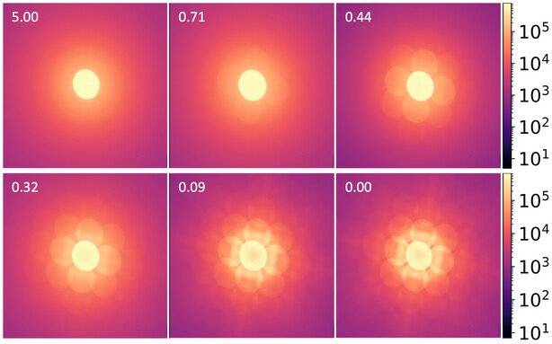
Figure 1: Electron diffraction patterns from silicon at six focused ion beam doses, each the sum of 10,000 diffraction patterns and shown on a logarithmic scale from 10¹ to 10⁵ counts. The number in each panel is the dose in ions per nm²; 0.00 is pristine silicon. Recorded on a QUADRO in a TESCAN TENSOR at 100 keV. Reproduced from Masteghin et al., Small Methods 2026 [1].
Solving the structure of a crystal grown inside a microalga, on an ELDICO ED-1
Wagner and colleagues showed in Nature Biotechnology [2] that the marine dinoflagellate Amphidinium carterae takes up a dozen nitrogen heterocycles from dilute solution and crystallizes them inside the cell, which turns a microalga into a source of crystals that are hard to grow in the lab. One of them, biogenic leucopterin, had no known structure. Its 3D electron diffraction (3D ED) data were recorded on an ELDICO ED-1 electron diffractometer, which adopts the QUADRO as the main detector. The experiment was done at 160 kV under continuous rotation: 0.5° and 0.5 s per frame, a −60° to +60° sweep in 120 s per crystal, at a dose rate of 0.01 electrons per Ų per second. This data, together with a unit cell obtained by X-ray based powder diffraction techniques, was enough to solve the structure of leucopterin hemihydrate. The 3D ED measurement itself was carried out by ELDICO Scientific AG.
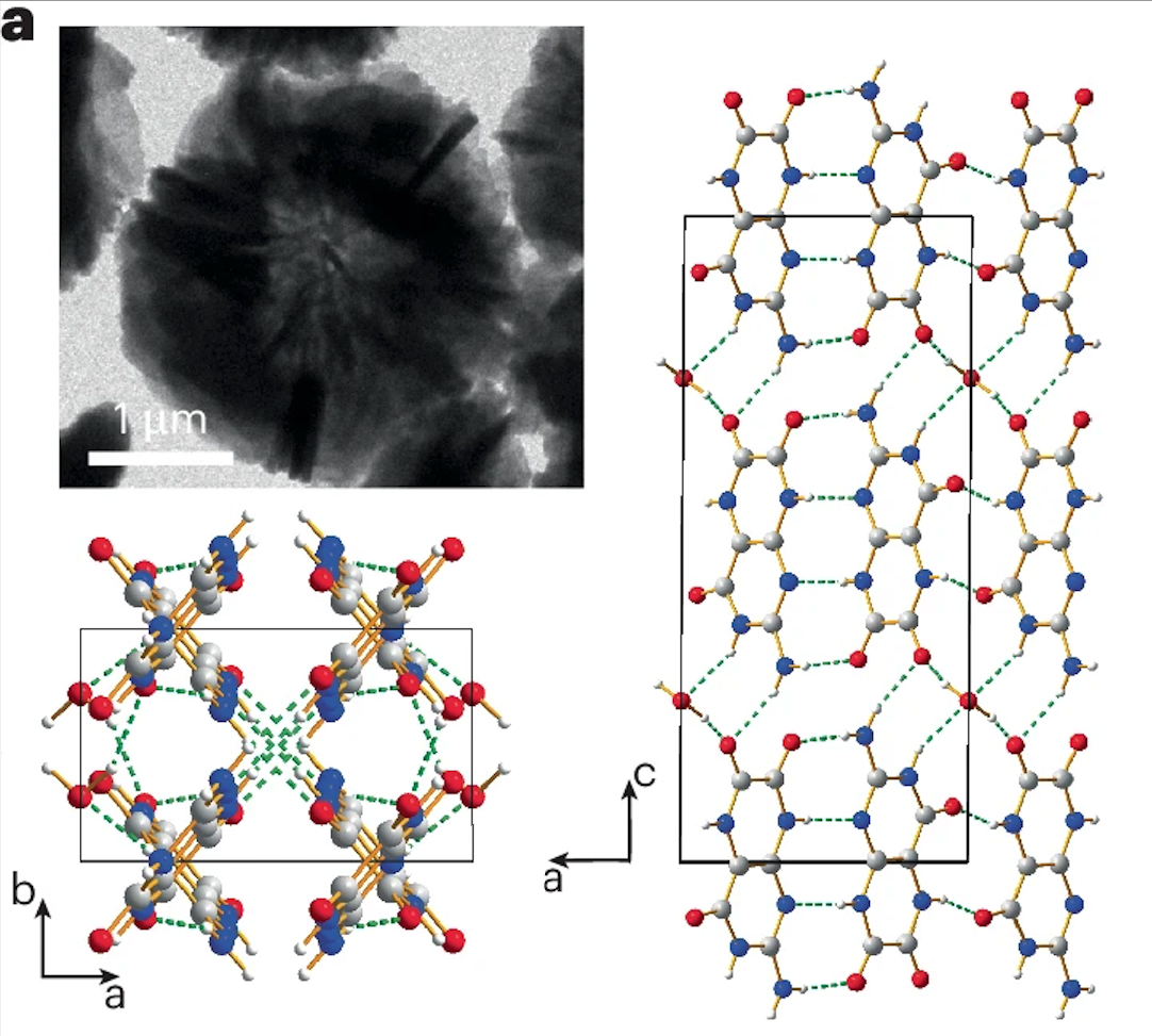
Figure 2: Crystal structure of biogenic leucopterin hemihydrate, solved from 3D electron diffraction data recorded on an ELDICO ED-1 with a QUADRO, together with a unit cell from synchrotron powder diffraction. Left: the criss-cross arrangement of hydrogen-bonded chains, viewed along the c axis. Right: leucopterin chains and water molecules, viewed along the b axis. Structure drawings from Fig. 4a of Wagner et al., Nature Biotechnology 2026 [2].
Watching a Mott switch operate in a home-built ultrafast TEM
Pofelski and colleagues built an all-electrical pump-probe ultrafast TEM: a modified JEOL JEM-2100F with an RF stripline pulser developed by Brookhaven National Laboratory and Euclid Techlabs, no laser, and electrical excitation from 1 Hz to 10 GHz [3]. In Nature Communications they used it to watch a working two-terminal VO₂ device switch, following the metallic filament from nucleation under the electrodes through growth at 4.54 nm/ns to coalescence and dissolution. They also showed that structural recovery, at 107 ± 21 ns, rather than the forward transition at 36 ± 10 ns, sets the frequency ceiling for such devices. Everything was recorded stroboscopically on a QUADRO, 5 s per bright-field image and 1 s per diffraction pattern, with each bright-field image summing about 5 million electrical cycles at a beam current density of only 0.36 A/m2 for the MHz series.
The authors put the detector's role plainly: "Utilizing a single-electron-sensitivity direct electron detector, we can capture the extremely weak signals associated with the propagating phase front." The 2.2 ns time resolution belongs to the pulser, and what the detector contributed was counting the few electrons that carried the signal.
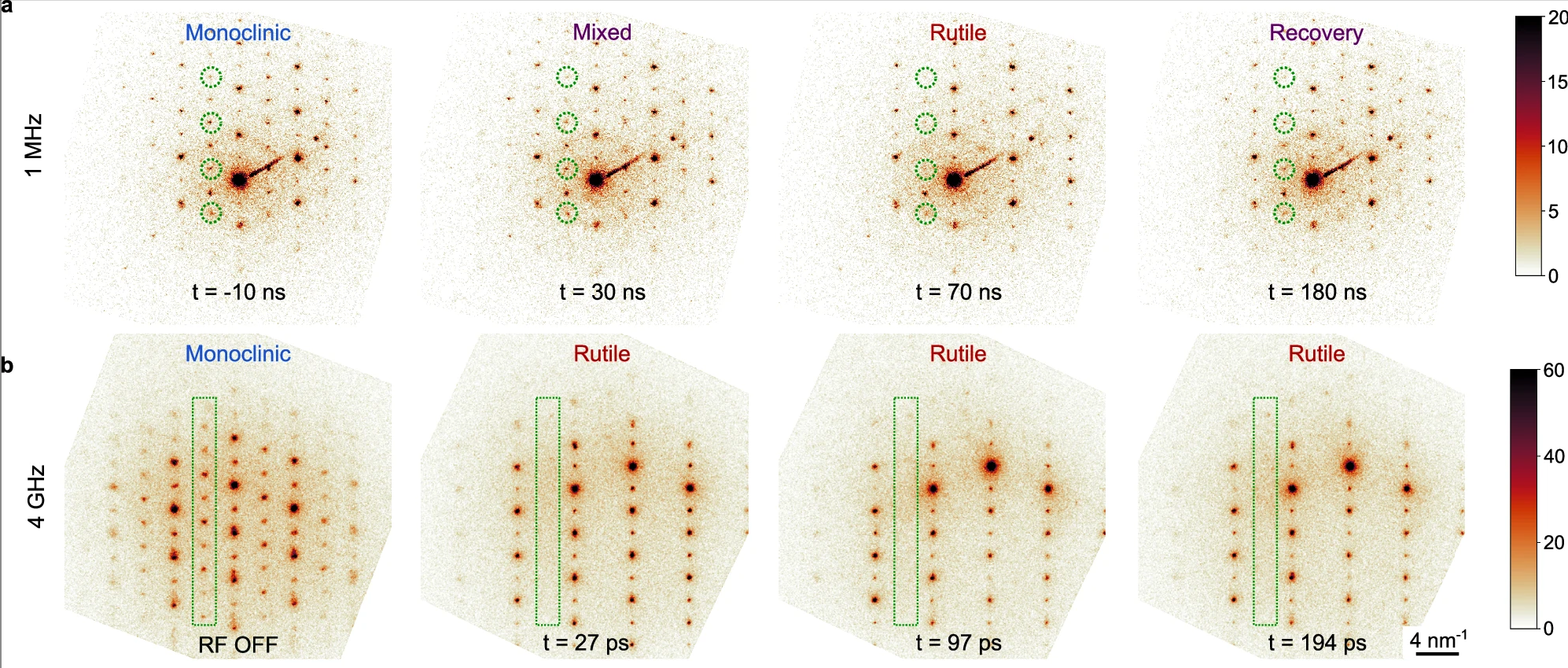
Figure 3: Stroboscopic electron diffraction patterns from a working VO₂ device under electrical excitation at 1 MHz (top row) and 4 GHz (bottom row), recorded on a QUADRO. The color scale is in electron counts and is saturated to bring out the weak reflections of the monoclinic phase, marked in green. Times are delays relative to the excitation. Panels a and b of Fig. 2, reproduced from Pofelski et al., Nature Communications 2026 [3].
Sub-ångström ptychography in a 20 keV Hitachi T-SEM
Blackburn and colleagues reached a Fourier ring correlation resolution of 0.67 Å by ptychography in a scanning electron microscope at 20 keV, with no aberration corrector, and published it in Nature Communications [4]. The microscope was a modified Hitachi SU9000 with a cold field-emission gun, an immersion objective and one added projector lens. Below its bright-field detector sat a QUADRO that had been optimized for operating in this energy range. The gold-on-amorphous-carbon dataset behind the 0.67 Å figure was a 90 × 90 grid at 0.5 nm steps and 85 pA, acquired in 40.5 s at 200 frames per second with no deadtime between frames. The authors name the low-energy-optimized hybrid direct electron detector as one of the four things that made the result possible.
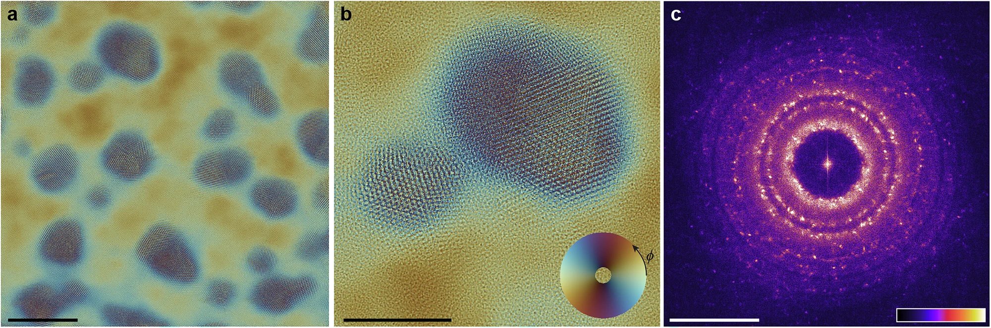
Figure 4: Ptychographic reconstruction of gold particles on amorphous carbon at 20 keV in a modified Hitachi SU9000 SEM, from diffraction patterns recorded on a modified QUADRO. (a) Reconstructed exit wave, scale bar 10 nm. (b) Enlarged region with two merged, twinned particles, scale bar 5 nm; the color wheel encodes phase as angle and amplitude as radius. (c) Fourier transform of the reconstruction, scale bar 1 Å⁻¹. Reproduced from Blackburn et al., Nature Communications 2025 [4].
A Single Detector for Shifting Research Priorities
These applications illustrate a broader pattern in modern electron microscopy: scientific questions rarely stay within the boundaries of a single technique. Moving between real-space imaging, high-speed 4D STEM, 3D electron diffraction, and low-dose methods often exposes the constraints of operating multiple single-purpose detectors.
Integrating a single, multi-modal direct electron detector addresses these constraints directly. For existing installations, adding QUADRO provides a practical path to significantly expand your lab’s experimental scope - bringing advanced diffraction, high dynamic range, and single-electron sensitivity to a microscope you already rely on, without the capital investment of a new instrument.
For labs evaluating new microscope purchases, choosing a multi-modal detector like QUADRO provides a cost-effective alternative to mounting multiple specialized devices. It integrates seamlessly across all major OEM platforms, equipping your instrument for a broad range of diffraction and imaging techniques from the moment it is installed. Paired with software like Novena Acquire, switching between real-space imaging and 4D STEM becomes a seamless part of your daily workflow rather than a hardware limitation.
With more than 25 peer-reviewed publications spanning 3D ED, in-situ work, ultrafast studies, and ptychography, QUADRO is designed to adapt as your research evolves. If you are exploring how to expand your current capabilities or want to discuss whether QUADRO fits your specific microscope setup and application goals, our application scientists are here to help you evaluate the best path forward.
References
[1] Masteghin, M. G. et al. Quantifying the Full Damage Profile of Focused Ion Beams via 4D-STEM Precession Electron Diffraction and PSNR Metrics. Small Methods 10, e02258 (2026). https://doi.org/10.1002/smtd.202502258
[2] Wagner, A. et al. Harnessing microalgae for the biosynthesis of molecular crystals. Nature Biotechnology (2026). https://doi.org/10.1038/s41587-026-03006-6
[3] Pofelski, A. et al. Switching speed limits in electrically driven VO₂ structural Mott–Peierls transition. Nature Communications 17, 3139 (2026). https://doi.org/10.1038/s41467-026-69904-0
[4] Blackburn, A. M. et al. Sub-ångström resolution ptychography in a scanning electron microscope at 20 keV. Nature Communications 16, 8977 (2025). https://doi.org/10.1038/s41467-025-64133-3